| the structure of CCDs |
|
Having looked at the physics of semi-conductors, we are now in a position to understand the structure of CCDs. There are two types, buried channel and surface channel. The surface channel device is the simplest CCD structure, but suffers from poor charge-handling performance as the electrons are stored and transfered close to the surface of the crystal, where the many irregularities and defects present cause charge traps. Surface-channel CCDs will not be considered further here. Instead, almost all scientific CCDs are buried-channel devices, which employ a p-n junction to bury the depletion region well below the silicon surface. A schematic of a buried-channel CCD pixel is shown in figure 103.
| figure 103: |
Schematic
cross-section through a CCD pixel.
|
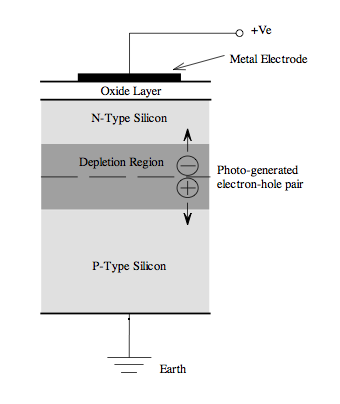
The bottom layer is a semi-conductor substrate, composed of a p-type silicon layer and an n-type silicon layer, i.e. a p-n junction. Over this is grown a thin layer of silicon dioxide, which is an insulator. On top of this is placed a metal electrode or gate, made of a transparent material known as polysilicon. The entire structure is known as a MOS capacitor, as it is composed of layers of, from top-to-bottom, Metal, Oxide and Semi-conductor.
By grounding the p-type silicon substrate and applying a positive voltage to the n-type layer, the p-n junction is reverse biased, widening the depletion region and creating a potential well in the n-type silicon that confines the electrons in the vertical direction in figure 103 (for more detail, see figures 6.12a,b of McLean, where it should be noted that in actual fact a separate positive voltage is applied to the electrode and the n-type silicon). Incident light generates electron-hole pairs in the depletion region, and the electrons migrate upwards into the n-type silicon layer where they are trapped in the vertical direction by the potential well. The electrons are therefore able to build up, with the amount of negative charge directly proportional to the level of incident light. The depth of the electron-collection layer (or buried channel) in the silicon can be controlled by altering the positive voltage on the electrode at the surface.
Note that it is important for the depletion region to permeate throughout as much of the thickness of the silicon as possible. This is because the depletion region is devoid of electrons, and hence any electrons that then appear in the potential well in the n-type silicon can safely be assumed to have been produced by incident photons. A thicker depletion region also ensures that there are no field-free regions in the silicon, as any photons striking such regions would be able to diffuse in a random manner away from the point of generation and either recombine with a hole and so not be counted, or be collected by the wrong pixel.
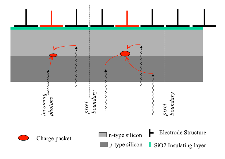
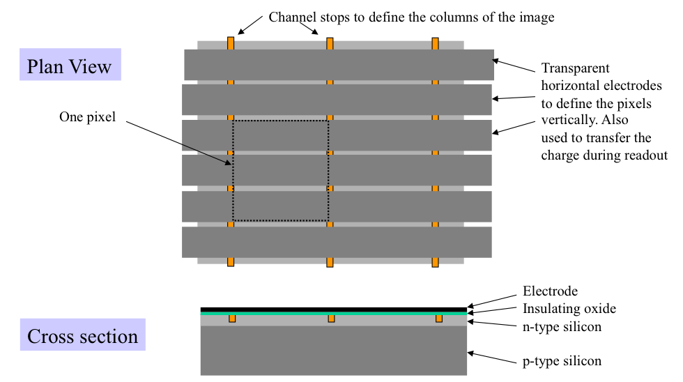
To create an array of CCD pixels, some means of isolating the charge packets held under each pixel is required. To prevent the collected charge from moving left and right in figure 103, a strip of insulator is implanted on either side, in structures known as channel stops. In the other dimension, the charge packet is held in place by splitting the electrode into a triplet, with the central electrode held at a more positive potential than the two on either side. Together, the channel stops and the electrode triplet define the pixel, as shown in figure 104.
| figure 104: |
Left: schematic cross-section
through three pixels of a CCD, showing how the charge packets in each pixel
are confined in the left-right direction by setting the central electrode
(red) of a triplet to a higher positive voltage.
Right: schematic of a small
portion of a CCD. The combination of channel stops and triplet electrode
structure is used to confine the charge packets in each pixel in both the
x and y directions.
|
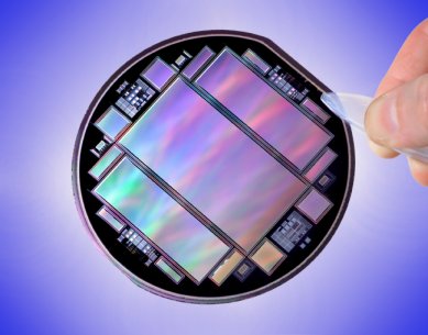
CCDs are manufactured on silicon wafers using the same
photo-lithographic techniques used to manufacture computer
chips. Scientific CCDs are very big - only a few can be fitted onto a
wafer, as shown in the left-hand panel of figure
105. This is the main reason why CCDs are so costly - large-format,
science-grade CCDs cost many tens of thousands of pounds. Electrical
connections are made to the outside world via a series of bond pads and
thin gold wires positioned around the chip periphery, as shown in the
central and right-hand panel of figure 105.
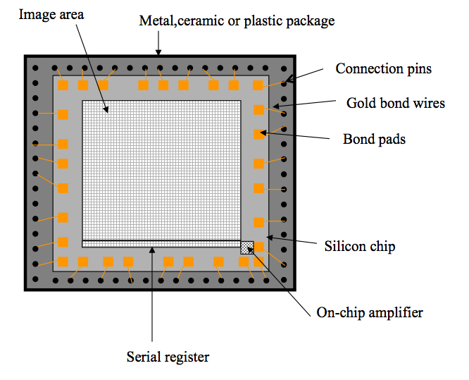
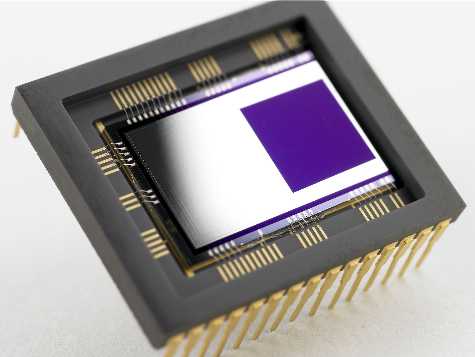
| figure 105: |
Left: photograph
of a 6" silicon wafer with three large CCDs and assorted smaller devices.
Centre: schematic showing
how CCDs are packaged. Right:
photograph showing an
E2V CCD97 package.
|